Ultrapure Water System for Electronics Industry: Complete Guide to System Overview and Key Characteristics 2026
What makes an ultrapure water system for the electronics industry fundamentally different from standard industrial water treatment systems? This comprehensive guide explains the overview, performance characteristics, system architecture, and water quality standards that define ultrapure water systems designed for semiconductor, integrated circuit, LCD, PCB, and other electronic device manufacturing applications. Understanding the ultrapure water system for electronics industry is essential for selecting, designing, and operating water purification equipment that meets the most demanding manufacturing requirements.
*Last Updated: May 2026 | Industry-Verified Standards
Why This Guide Matters
The global ultrapure water market for electronics manufacturing was valued at approximately USD 8.3 billion in 2024 and is projected to reach USD 15.7 billion by 2034, growing at a CAGR of 6.6%. Semiconductor fabrication alone consumes 500-2,000 gallons of ultrapure water per 300mm wafer per fabrication layer, with a single advanced fab using 10-20 million gallons per day. The water quality specifications are extraordinarily stringent — resistivity must be maintained above 18.15 Mohm-cm, TOC below 1 ppb, dissolved oxygen below 1 ppb, and particles above 0.05 micron below 100 counts per liter. A properly designed ultrapure water system for the electronics industry must achieve and maintain these specifications continuously, as any deviation can cause catastrophic yield losses in chip fabrication. For an in-depth introduction to EDI and electrodeionization, refer to our guide on electrodeionization (EDI) in clean water production.
Key Industry Trends (2026 Update)
- Sub-3nm node water demands intensifying — Advanced fabrication nodes below 3 nm require ultrapure water with TOC below 0.5 ppb and dissolved oxygen below 0.5 ppb, driving adoption of advanced UV oxidation, membrane degasification, and real-time process monitoring systems.
- Water recycling and reclaim becoming essential — With fabs consuming 10-20 million GPD, water recycling rates of 75-90% are now standard in new facilities, requiring sophisticated reclaim treatment trains and dedicated distribution systems for different water grades.
- RO-EDI hybrid systems dominating new installations — The vast majority of new electronics-industry ultrapure water systems now use RO-EDI hybrid rather than RO-ion exchange, eliminating chemical regeneration waste and enabling continuous 18.2 Mohm-cm operation without downtime for resin replacement.
- Digital twin and AI optimization emerging — Leading-edge fabs are implementing digital twin models of their ultrapure water systems that use machine learning to predict membrane fouling, optimize chemical dosing, and schedule automated CIP cleaning, reducing unplanned downtime by 40-50%.
1. What Is an Ultrapure Water System for the Electronics Industry?
Overview and Significance
An ultrapure water system for the electronics industry is a multi-stage water treatment facility specifically engineered to produce water of the highest purity — typically 18.2 Mohm-cm resistivity with sub-ppb levels of TOC, dissolved oxygen, silica, bacteria, and particles — for use in semiconductor, integrated circuit (IC) chip and packaging, liquid crystal display (LCD), high-precision printed circuit board (PCB), optoelectronic device, microelectronics, and large-scale and ultra-large-scale integrated circuit manufacturing processes. These systems produce massive quantities of pure water, high-purity water, and ultrapure water to clean semi-finished and finished products at every stage of the manufacturing process. As integrated circuit integration increases and line widths narrow, the water quality requirements become exponentially more stringent — a trend that pushes the boundaries of water treatment technology with each new fabrication node. For a detailed overview of water quality standards and applications, see our article on how EDI replaces mixed bed technology in modern systems.
Water Quality Grade Classification
The electronics industry classifies water quality into five distinct levels based on resistivity, each corresponding to specific manufacturing applications: Grade 1 (18 Mohm-cm) — the highest standard, required for sub-micron IC fabrication, wafer cleaning, and critical process steps; Grade 2 (15 Mohm-cm) — suitable for general semiconductor processing and LCD manufacturing; Grade 3 (10 Mohm-cm) — used for PCB manufacturing, optoelectronic device cleaning, and less critical semiconductor steps; Grade 4 (2 Mohm-cm) — adequate for certain chemical preparation and general electronics washing; and Grade 5 (0.5 Mohm-cm) — the minimum standard for non-critical rinsing and equipment cooling applications. The Chinese Ministry of Electronics Industry recognizes these five industry levels as the standard classification framework for electronic water quality technology.
2. What Are the Key Components of an Electronics-Grade Ultrapure Water System?
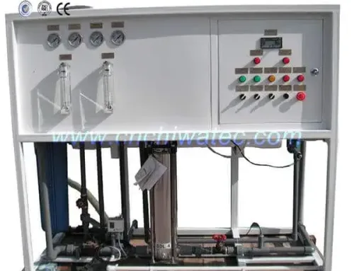
Pretreatment System Components
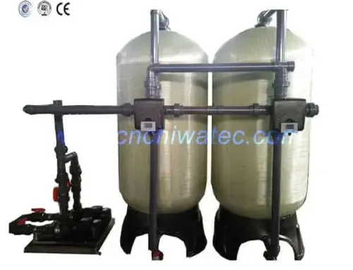
The pretreatment section of an ultrapure water system for the electronics industry typically consists of: a multi-media filter (graded quartz sand and anthracite) for removing suspended solids above 20 microns; an activated carbon filter for chlorine, chloramine, and organic compound removal (essential for protecting downstream RO membranes from oxidation); a sodium ion water softener for calcium and magnesium hardness removal (preventing scale formation on RO membranes); and a 5-micron precision security filter as the final particulate barrier before the RO stage. Each pretreatment component is sized with redundant capacity to allow online maintenance without interrupting ultrapure water production — a standard requirement for 24/7 semiconductor manufacturing operations. For a thorough analysis of EDI principles and system configurations, refer to our guide on EDI principle and its application in pure water clean production.
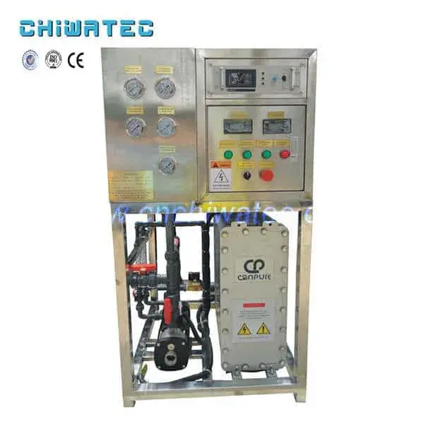
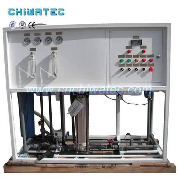
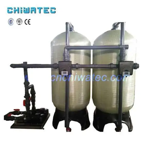
RO and EDI Main Treatment System
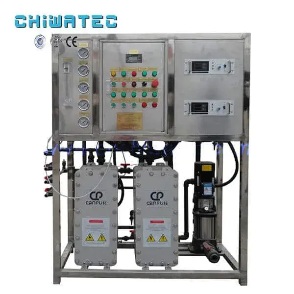
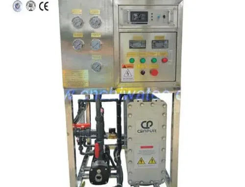
The main treatment section comprises the RO reverse osmosis host system and the EDI (electrodeionization) or ion exchange mixed bed polishing system. The RO system typically uses a two-pass configuration with low-energy TFC membrane elements, achieving 99.5% plus salt rejection and producing water with conductivity below 5 microsiemens/cm. The RO permeate then feeds the EDI module stack, where continuous electrodeionization removes residual ionic impurities to achieve the final resistivity target of 18.2 Mohm-cm. The EDI system operates without chemical regeneration — an important advantage for electronics manufacturing, where chemical handling and waste disposal present contamination risks and regulatory compliance burdens. The entire system includes raw water storage tanks, intermediate water tanks, RO pure water tanks, and ultrapure water storage tanks, each equipped with liquid level control systems and nitrogen blanketing to prevent atmospheric CO2 absorption.
Automation and Control Infrastructure
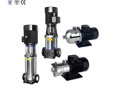
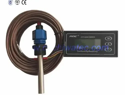
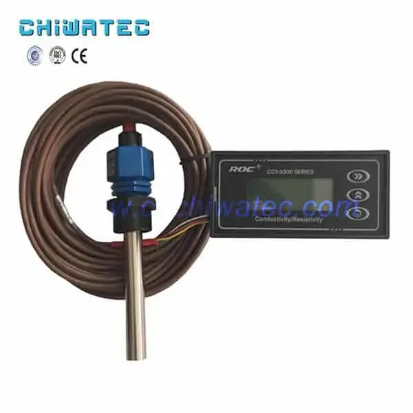
All high and low-pressure water pumps are equipped with high and low-pressure protection devices. The system includes online water quality detection and control instruments — typically including resistivity meters, TOC analyzers, dissolved oxygen meters, particle counters, and silica analyzers — providing real-time water quality monitoring at multiple points throughout the treatment train. The electrical control system uses PLC programmable controllers with HMI touchscreens, enabling fully unattended 24/7 operation. The control system manages automatic start-stop sequences, regeneration cycles (for mixed bed systems), chemical cleaning scheduling, and alarm management for any out-of-spec conditions.
3. What Are the Characteristics of Ultrapure Water Equipment in the Electronics Industry?
Performance and Reliability Characteristics
Electronics-grade ultrapure water equipment exhibits several distinguishing characteristics that set it apart from industrial or pharmaceutical water systems. Continuous ultra-high purity output — the system must deliver water at 18.2 Mohm-cm with TOC below 5 ppb (and below 1 ppb for advanced nodes) 24 hours per day, 365 days per year, with zero tolerance for quality excursions. Component redundancy — critical components including pumps, RO vessels, EDI modules, UV units, and monitoring instruments are configured with N+1 redundancy, allowing maintenance without production interruption. Material compatibility — all wetted materials (PVDF, PTFE, high-purity PVC, 316L stainless steel with electropolished surfaces) are selected to prevent leaching of contaminants into the ultrapure water stream. For a detailed comparison of treatment technologies, see our article on advantages of EDI technology compared with hybrid ion exchange.
System Design and System Integration
The system design incorporates several advanced features: modular skid-mounted construction for factory testing and rapid on-site installation, recirculation loops with point-of-use (POU) polishing to maintain water quality throughout the distribution network, UV oxidation (185 nm) for TOC reduction below the analyzer detection limit, membrane degasification for dissolved oxygen removal to below 1 ppb, and 0.04-micron (40 nm) point-of-use ultrafiltration for final particle removal. The complete system is designed with a total system approach, where each component is selected and integrated to achieve the final water quality target rather than each component operating independently.
4. How Does the System Control Water Quality at Multiple Points?
Online Monitoring and Quality Assurance
In an ultrapure water system for the electronics industry, continuous online monitoring is mandatory at multiple points throughout the treatment train. Critical monitoring points include: after the RO system — conductivity measurement to verify 95-99% rejection; after EDI — resistivity measurement (typically 16-18 Mohm-cm); after UV oxidation — TOC measurement (below 1-5 ppb); after membrane degasification — dissolved oxygen measurement (below 1 ppb); and at each point of use — resistivity, TOC, particle counts, and silica measurement. All monitoring instruments are calibrated against NIST-traceable or equivalent standards on a scheduled basis, with automatic data logging for compliance verification and trend analysis. Xi’an CHIWATEC integrates comprehensive online monitoring packages into all electronics-industry ultrapure water systems.
Automatic Diversion and Alarm Systems
Any deviation from water quality specifications triggers automatic diversion of out-of-spec water to drain or reclaim, preventing contaminated water from reaching the manufacturing process. The system includes: resistivity-based automatic diversion valves that close when resistivity drops below the setpoint (typically 18.0-18.15 Mohm-cm), TOC-based alarms that alert operators to organic breakthrough, particle counter alarms that indicate filter integrity issues, and common alarm outputs integrated with the fab’s facility monitoring system (FMS) for immediate operator notification. This multi-layered quality assurance approach ensures that only water meeting the most stringent specifications reaches the manufacturing process.
5. What Water Quality Standards Apply to Electronics Manufacturing?
SEMI and ASTM Standards
The electronics industry follows several internationally recognized water quality standards. The SEMI (Semiconductor Equipment and Materials International) standards — particularly SEMI C1 for chemical specifications and SEMI F63 for ultrapure water — define the most comprehensive requirements. The ASTM D5127-07 (Standard Guide for Ultra-Pure Water Used in the Electronics and Semiconductor Industry) specifies: Type E-1.1 for the most critical applications (18.2 Mohm-cm, TOC below 5 ppb, DO below 1 ppb, silica below 0.5 ppb, bacteria below 0.1 CFU/100 mL, particles above 0.05 micron below 100/L), through to Type E-IV for less critical uses. These standards are regularly updated to reflect the increasingly stringent requirements of advanced manufacturing processes. For information on system maintenance, see our EDI ultrapure water equipment problems and solutions guide.
Water Quality Verification Protocols
Ensuring compliance with these stringent standards requires rigorous verification protocols. Online instruments provide continuous monitoring, but periodic grab sample testing is also required for parameters that cannot be monitored online (such as specific metals by ICP-MS or specific organic compounds by LC-MS). Sampling frequency ranges from daily for resistivity and TOC to monthly or quarterly for comprehensive metals panels. Sample collection must follow strict protocols to prevent contamination during the sampling process, using dedicated sample points with continuous purge flow and specific collection container requirements.
6. How Does the System Architecture Support 24/7 Reliability?
Redundant Component Configuration
The ultrapure water system for the electronics industry is designed with full N+1 redundancy for all critical components. The pretreatment section includes dual-media filters that can operate independently while one is backwashed, dual-carbon vessels for chlorine removal, and dual-precision filters that can be changed without system shutdown. The RO section may include multiple membrane vessels with one spare, or a two-pass configuration where the second pass can accept higher feed TDS if the first pass is compromised. EDI modules are arranged in a lead-lag configuration or multiple parallel stacks, where individual stacks can be isolated for maintenance while the remaining stacks maintain production. This architectural approach ensures the system achieves the 99.999% plus uptime required by semiconductor manufacturing operations.
Distribution System Design
The ultrapure water distribution system is as critical as the treatment system itself. Key design features include: recirculation loops that maintain constant flow velocity (typically 1.5-3 m/s) to prevent stagnation and bacterial growth, all-stainless-steel or PVDF piping with orbital-welded joints to eliminate dead legs, continuously operating recirculation pumps with redundant backup, and point-of-use polishing stations that include mixed-bed ion exchange cartridges and 0.04-micron ultrafilters for final polishing immediately before the manufacturing process. The distribution system is designed to maintain water quality from the treatment plant to every point of use in the fab.
7. What Makes EDI the Preferred Polishing Technology for Electronics?
Advantages Over Mixed-Bed Ion Exchange
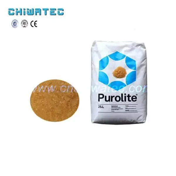
EDI (electrodeionization) has become the preferred final polishing technology for electronics-grade ultrapure water systems due to several critical advantages over traditional mixed-bed ion exchange. Continuous operation — EDI operates continuously without the batch regeneration cycles required by mixed beds, eliminating downtime for regeneration and the associated chemical handling, storage, and waste disposal requirements. Consistent effluent quality — EDI consistently produces water at 16-18.2 Mohm-cm regardless of feed water variability, while mixed-bed effluent quality degrades as the resin approaches exhaustion between regenerations. No chemical regeneration — EDI uses electrical current to continuously regenerate the ion exchange resin internally, eliminating the need for acid and caustic chemicals that pose safety and environmental hazards. Xi’an CHIWATEC provides complete RO-EDI system designs optimized for electronics manufacturing. For a side-by-side comparison, see our performance comparison of mixed bed and EDI.
Cost and Environmental Benefits
While the initial capital cost of EDI is higher than equivalent mixed-bed systems, the total cost of ownership over a 10-year period is typically 20-30% lower when all factors are considered: elimination of chemical costs (acid and caustic), elimination of chemical waste disposal costs, reduced labor for regeneration operations, reduced downtime for regeneration cycles, and longer component life with fewer replacement cycles. Additionally, EDI eliminates the safety risks associated with chemical handling — an important consideration for facilities that must maintain stringent safety and environmental compliance standards.
8. What Specific Electronics Manufacturing Processes Use Ultrapure Water?
Semiconductor Wafer Fabrication
Semiconductor wafer fabrication — the most demanding application — uses ultrapure water at virtually every process step. In wafer cleaning, ultrapure water removes chemical residues, particles, and metallic contaminants between process steps — a single wafer may be cleaned 50-100 times during fabrication. In wet etching and chemical mechanical planarization (CMP), ultrapure water serves as the dilution and rinsing medium for etch chemicals and CMP slurries. In photolithography, ultrapure water is used for optics cleaning and wafer rinse between resist coating, exposure, and development steps. The total water consumption for a 300mm wafer fab processing 40,000 wafer starts per month ranges from 10,000-20,000 cubic meters per day (2.6-5.3 million gallons per day). For a comprehensive discussion of system process flow, see our article on process flow and application fields of ultrapure water in the electronics industry.
Flat Panel Display Manufacturing
LCD and OLED display manufacturing requires ultrapure water for substrate cleaning, chemical dilution, etching rinse, and final product cleaning. Display fabrication uses significant water volumes — a Gen 8.5 glass substrate (2200 by 2500 mm) requires 50-100 liters of ultrapure water per substrate pass, with total fab consumption reaching 5,000-10,000 cubic meters per day. The water quality requirements for display manufacturing are similar to semiconductor requirements, although TOC specifications may be slightly relaxed for less critical process steps.
9. What Are the Key Considerations for Selecting an Electronics-Grade UPW System?
Feed Water Quality and Site Assessment
Proper system design begins with a comprehensive feed water analysis covering TDS, hardness, alkalinity, silica, TOC, bacterial counts, iron, manganese, and seasonal variability. The feed water source — municipal, well, or surface water — determines the pretreatment complexity required. Electronics manufacturing facilities located in areas with challenging feed water may require additional pretreatment stages such as lime softening, ultrafiltration, or EDR (electrodialysis reversal) before the main RO-EDI treatment train.
Capacity and Expansion Requirements
Design capacity must account for: current manufacturing water consumption plus planned expansion (typically 20-50% future capacity is incorporated in the initial design), peak demand versus average demand — semiconductor manufacturing creates instantaneous flow demands that may be 2-3 times the average, water quality distribution loops — different process areas may require different water quality grades (18.2, 15, 10 Mohm-cm), and reclaim and recycling infrastructure — modern fabs reclaim 75-90% of used water, requiring separate reclaim treatment and distribution systems. CHIWATEC provides turnkey ultrapure water system design and installation services for the electronics industry, from initial feasibility studies through commissioning and validation.
10. How to Maintain and Operate an Electronics-Grade Ultrapure Water System?
Preventive Maintenance Program
A comprehensive preventive maintenance program is essential for maintaining the consistent water quality required by electronics manufacturing. Daily tasks include verifying online resistivity readings, checking EDI module operating parameters (voltage, current, flow rates), reviewing TOC analyzer trends, and inspecting for leaks. Weekly tasks include calibrating online instruments against standards, checking chemical feed pump operation, and verifying recirculation loop flow rates. Monthly tasks include RO membrane performance normalization, EDI stack performance analysis, and particle counter verification. Quarterly tasks include total system sanitization, UV lamp replacement (typically every 8,000-12,000 hours), and comprehensive water quality analytical testing. For guidance on maintaining EDI systems, see our how to maintain EDI ultrapure water equipment.
Managing Membrane and EDI Stack Replacement
RO membrane elements in electronics-grade systems typically require replacement every 3-5 years, depending on feed water quality and pretreatment effectiveness. EDI module stacks have a longer service life, typically 5-10 years, with the ion exchange resin and membranes gradually degrading from continuous electrical and chemical stress. Replacement planning should be integrated with semiconductor fab maintenance schedules to coordinate water system downtime with planned fab maintenance shutdowns. Spare EDI stacks and RO membrane elements should be maintained in inventory to minimize downtime in case of unexpected failure.
Conclusion
The ultrapure water system for the electronics industry represents the pinnacle of water treatment technology, producing water of extraordinary purity — 18.2 Mohm-cm resistivity with sub-ppb levels of TOC, dissolved oxygen, silica, bacteria, and particles — that is essential for manufacturing the semiconductor, display, and electronic devices that power the modern world. These systems combine comprehensive pretreatment, reverse osmosis, electrodeionization, UV oxidation, membrane degasification, and point-of-use polishing with sophisticated automation, redundant component configuration, and continuous online monitoring to achieve the 99.999% plus uptime and consistent water quality that semiconductor and electronics manufacturing demands. As fabrication nodes continue to shrink and new technologies such as advanced packaging, 3D NAND, and GaN semiconductors emerge, the water quality requirements will only become more stringent. For expert guidance on designing, selecting, or upgrading an ultrapure water system for your electronics manufacturing facility, contact Xi’an CHIWATEC today at [email protected] or [email protected], or reach us via WhatsApp.
Frequently Asked Questions
Q1: Why does the electronics industry need such high-purity water?
Semiconductor and electronics manufacturing involves creating structures with features measured in nanometers — billionths of a meter. A single particle of 0.1 micron deposited on a wafer during manufacturing can render an entire die non-functional, potentially causing losses of thousands of dollars per wafer. Similarly, ionic contamination at the part-per-trillion level can alter the electrical properties of transistors, reducing performance or causing device failure. Ultrapure water is the universal cleaning and rinsing medium in electronics fabrication because it removes contaminants without adding any of its own.
Q2: What is the difference between ultrapure water and distilled water?
Distilled water typically has resistivity of 0.5-1 Mohm-cm and TOC of 200-500 ppb, while electronics-grade ultrapure water has resistivity above 18 Mohm-cm and TOC below 1-5 ppb — several orders of magnitude purer. Distillation removes inorganic ions effectively but does not remove organic compounds well and can introduce CO2 and volatile organic compounds during the condensation process. Ultrapure water production uses a multi-stage approach (RO + EDI + UV + degasification) specifically designed to remove all classes of contaminants — inorganic, organic, particulate, bacterial, and gaseous — to the sub-ppb level.
Q3: How much does an electronics-grade ultrapure water system cost?
The cost of an ultrapure water system for electronics manufacturing varies widely based on capacity, water quality requirements, and site-specific factors. A small-capacity system (10-50 m3/h) for an assembly or test facility may cost USD 500,000-2 million, while a complete system for a 300mm wafer fab (5,000-10,000 m3/h) can cost USD 10-50 million including distribution piping, reclaim systems, and control infrastructure. Operating costs for a large fab ultrapure water system range from USD 0.10-0.30 per cubic meter including energy, chemicals, consumables, and maintenance.
Q4: How is water quality monitored in real time?
Continuous online monitoring is performed using: resistivity/conductivity sensors with temperature compensation, TOC analyzers using UV persulfate oxidation or conductivity differential methods, dissolved oxygen sensors using fluorescence quenching technology, laser-based particle counters with sensitivity down to 0.05 micron, and silica analyzers using colorimetric molybdate method. All instruments are networked to the central control system with automatic data logging and alarm management. Calibration verification using standards is performed on a scheduled basis, and any out-of-spec condition triggers automatic product water diversion.
Q5: Can ultrapure water be stored for later use?
Ultrapure water cannot be effectively stored for extended periods — its high purity makes it chemically aggressive, dissolving contaminants from any material it contacts and absorbing CO2 from ambient air. Resistivity drops from 18.2 Mohm-cm to below 1 Mohm-cm within hours of exposure to air. For this reason, ultrapure water is typically stored in nitrogen-blanketed storage tanks with minimal headspace, continuously recirculated through UV and polishing loops, and used within minutes of production. The distribution system is designed to maintain purity through recirculation rather than relying on large-volume storage.
Related Resources and Further Reading
Do you have a water treatment project we can help with
* Designing,machining,installing,commissioning, customize and one-stop service
