Semiconductor Ultrapure Water Process: Complete Guide to UPW for Wafer Fabrication 2026
Semiconductor manufacturing demands the highest purity water of any industry, requiring ultrapure water (UPW) at 18.2 MΩ·cm with TOC below 1 ppb for critical wafer fabrication steps. The semiconductor ultrapure water process must eliminate virtually all contaminants — particles, dissolved ions, organic compounds, bacteria, and dissolved gases — to prevent yield-killing defects on nanometer-scale circuits. This guide covers the complete semiconductor ultrapure water process, from traditional RO plus mixed bed to advanced RO-EDI configurations, helping fabs select the optimal UPW system. CHIWATEC provides custom-engineered ultrapure water equipment for semiconductor facilities worldwide.
Why Semiconductor Manufacturing Requires Specialized Ultrapure Water
In semiconductor fabrication, ultrapure water is the most heavily used process chemical, consumed in wafer cleaning, rinsing, chemical mechanical planarization (CMP), and wet etching steps. A typical 300 mm wafer fab uses 4,000-8,000 m³ of UPW per day. Even trace contaminants cause catastrophic defects:
- Particles at 0.05 μm — Cause shorts between circuit lines on advanced nodes (7 nm and below)
- Dissolved ions (Na⁺, K⁺, Cl⁻) — Dope unintended regions, altering transistor threshold voltages
- TOC above 1 ppb — Creates organic residues that interfere with photoresist adhesion and gate oxide integrity
- Dissolved oxygen — Promotes native oxide growth on silicon surfaces, degrading device performance
- Bacteria — Release endotoxins and organic byproducts that contaminate rinse baths
The semiconductor ultrapure water process must consistently deliver water meeting SEMI C57-0310 and ASTM D5127 standards to achieve acceptable die yields.
Semiconductor Ultrapure Water Quality Specifications
| Parámetro | Especificación | Test Method |
|---|---|---|
| Resistivity at 25°C | ≥18.2 MΩ·cm | In-line resistivity meter |
| Total Organic Carbon (TOC) | ≤1 ppb (advanced: ≤0.5 ppb) | UV oxidation + conductivity |
| Particle count (>0.05 μm) | ≤1 particle/L | Liquid particle counter |
| Dissolved Oxygen (DO) | ≤1 ppb (advanced: ≤0.1 ppb) | Membrane-based DO sensor |
| Bacteria | ≤0.1 CFU/100 mL | Culture or ATP method |
| Silica (total) | ≤0.5 ppb | ICP-MS |
| Metals (each, e.g. Na, K, Fe) | ≤0.01 ppb | ICP-MS |
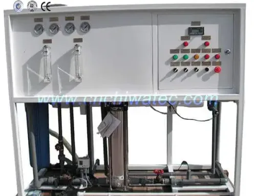
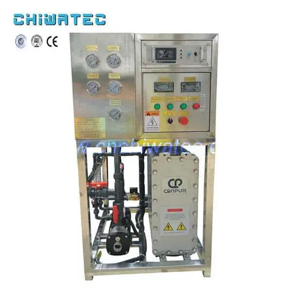
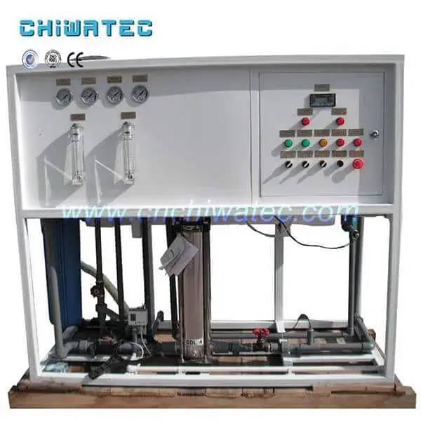
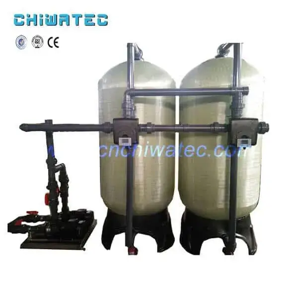
Traditional RO Plus Mixed Bed Process for Semiconductor Ultrapure Water
The traditional semiconductor ultrapure water process uses reverse osmosis followed by multiple stages of mixed bed ion exchange for final polishing:
Flow Sequence: Pretreatment System → RO System → Intermediate Tank → Coarse Mixed Bed → Fine Mixed Bed → Pure Water Tank → Pure Water Pump → UV Sterilizer → Polishing Mixed Bed → Precision Filter → Point of Use (≥18 MΩ·cm)
Key characteristics:
- RO removes 95-99% of dissolved solids before ion exchange polishing
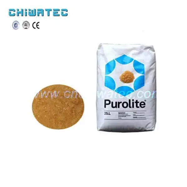
- Coarse and fine mixed beds handle the bulk deionization load in sequence
- Polishing mixed bed at the end achieves 18.2 MΩ·cm resistivity
- UV sterilizer at 254 nm (bacteria) and 185 nm (TOC reduction) maintains water quality in the storage loop
Limitations: Mixed bed regeneration requires periodic chemical handling (HCl + NaOH), generates acidic/alkaline waste, and causes temporary resistivity dips during regeneration cycles. For advanced semiconductor nodes, these dips can affect critical rinse steps.
Modern RO Plus EDI Technology for Semiconductor UPW
The latest semiconductor ultrapure water process replaces regenerable mixed beds with electrodeionization (EDI) for continuous, chemical-free polishing:
Flow Sequence: Pretreatment → Primary RO → Degasification → Secondary RO (optional) → EDI Module → UV TOC Reduction → Polishing Mixed Bed → Degasification Membrane → Point of Use (18.2 MΩ·cm, <1 ppb TOC)
Advantages over traditional mixed bed:
- Zero chemical regeneration — EDI uses DC electrical current to continuously regenerate internal resins
- Continuous operation — No regeneration downtime; consistent 18.2 MΩ·cm resistivity 24/7
- Lower TOC — EDI modules also remove ionized organic species, helping achieve ≤1 ppb TOC
- Compact footprint — EDI stacks replace multiple mixed bed vessels, saving cleanroom space
- Reduced environmental impact — No acid/alkali wastewater; lower carbon footprint
Most advanced semiconductor fabs (sub-14 nm nodes) now specify RO + EDI as the baseline semiconductor ultrapure water process, often with additional polishing steps such as UV TOC reduction, membrane degasification, and final mixed bed polishing.
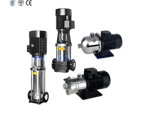
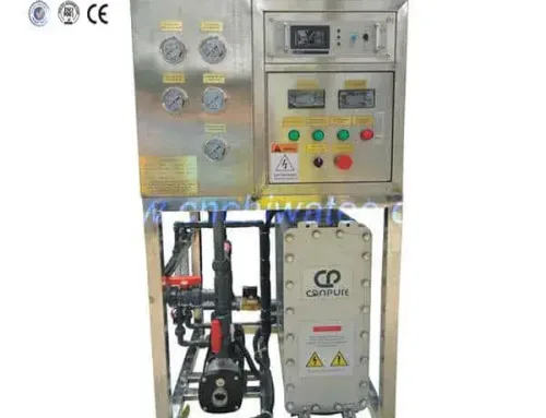
Critical Equipment in Semiconductor Ultrapure Water Systems
| Component | Función | Semiconductor Specification |
|---|---|---|
| RO System | Primary desalination, 95-99% rejection | Thin-film composite, 150-300 psi |
| EDI Module | Continuous deionization, no chemicals | Output ≥16 MΩ·cm, 50-300 VDC |
| UV TOC Reduction | Oxidize organic compounds | 185 nm wavelength, 500-1000 mJ/cm² |
| Membrane Degasification | Remove dissolved O₂, CO₂ | DO ≤1 ppb, hydrophobic membrane |
| Polishing Mixed Bed | Final resistivity boost to 18.2 MΩ·cm | Nuclear-grade resin, in-situ regeneration |
| Point-of-Use Filters | Final particle removal | 0.03-0.05 μm absolute rating |
How to Choose the Right Semiconductor Ultrapure Water Process
Selecting between traditional and modern configurations depends on the fab’s technology node, water volume, and environmental policies:
- Technology node: For mature nodes (≥28 nm), traditional RO + mixed bed may suffice. For advanced nodes (≤14 nm), RO + EDI with UV TOC reduction and membrane degasification is mandatory.
- Water volume: Fabs above 4,000 m³/day benefit most from EDI’s lower operating cost — the chemical savings from eliminating regeneration outweigh the higher capital investment within 2-3 years.
- Environmental compliance: Fabs under strict discharge permits should prioritize EDI to eliminate acid/alkali wastewater. Many Asian and European semiconductor clusters now mandate zero-chemical UPW systems.
- Space constraints: EDI stacks require 30-50% less floor space than equivalent mixed bed vessels — a critical advantage in expensive cleanroom environments.
CHIWATEC engineers complete UPW systems for semiconductor applications, from pretreatment through final polishing, with full validation support.
Frequently Asked Questions
What resistivity does semiconductor ultrapure water require?
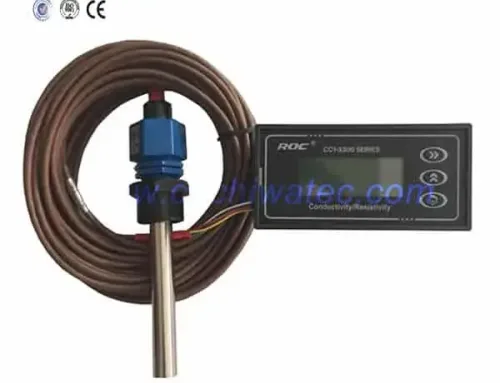
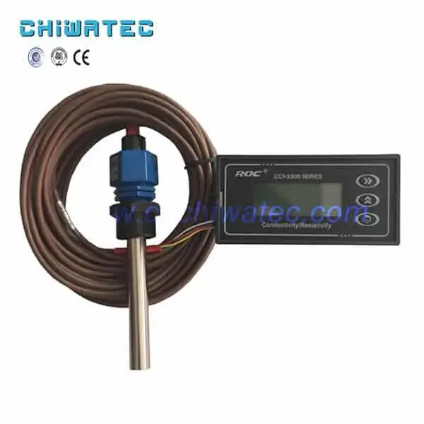
Semiconductor fabs require ≥18.2 MΩ·cm at 25°C, which represents the theoretical maximum resistivity of pure water. Readings below 18.0 MΩ·cm indicate ionic contamination that can affect device yields. In-line resistivity monitors continuously verify water quality at each point of use.
How does EDI achieve 18.2 MΩ·cm for semiconductor applications?
EDI alone typically produces water at 16-18 MΩ·cm. To reach 18.2 MΩ·cm, a polishing mixed bed is placed after the EDI module. Because the EDI effluent is already 99.9% pure, the polishing bed operates with extremely long regeneration cycles (6-12 months versus 2-7 days without upstream EDI).
What is the typical capital cost of a semiconductor ultrapure water system?
A complete semiconductor UPW system for a 300 mm fab (capacity 4,000-8,000 m³/day) typically costs $15-40 million, including pretreatment, RO trains, EDI stacks, UV systems, degasification, storage/distribution, and validation. Cost scales with flow rate and final water quality requirements.
How often do EDI modules need replacement in semiconductor service?
EDI module stacks typically last 5-8 years in semiconductor UPW service with proper pretreatment (RO permeate with conductivity <40 μS/cm). Key life-limiting factors include silica scaling, hardness breakthrough, and gradual resin degradation from repeated electrical cycling.
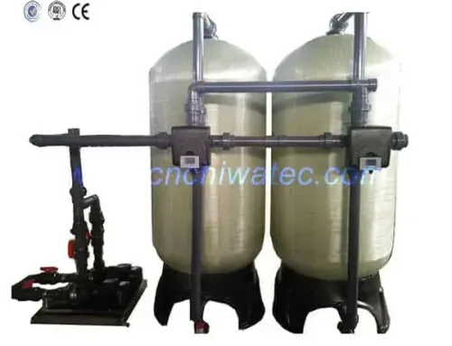
What pretreatment is required before the RO system?
Standard pretreatment includes multimedia filtration (particle removal), activated carbon (chlorine/organic removal), water softening (hardness removal), and 5 μm cartridge filtration. For surface water sources, additional steps may include coagulation, flocculation, and UF membrane pretreatment to achieve SDI <3.
Conclusion & Call to Action
Semiconductor manufacturing demands the highest purity water of any industry, and the semiconductor ultrapure water process must be meticulously designed to meet sub-ppb contamination limits. Modern RO + EDI systems offer chemical-free, continuous operation with consistent 18.2 MΩ·cm output — the preferred choice for advanced fabs worldwide. CHIWATEC provides complete one-stop service for semiconductor ultrapure water systems: designing, machining, installing, commissioning, and customization.
Correo electrónico: [email protected] o [email protected]
Related Resources and Further Reading
- Process Flow of Ultrapure Water Equipment in Electroplating Industry
- Electroplating Ultrapure Water Equipment Process: Complete Guide
- Process Flow of Ultrapure Water Equipment in Electronics Factory
- Laboratory Ultrapure Water Equipment Process: Complete Guide
- Ultrapure Water Purification System for Semiconductor Industry
¿Tiene un proyecto de tratamiento de agua con el que podamos ayudar?
* Diseño, mecanizado, instalación, puesta en marcha, personalización y servicio integral
